News

ELVIA PCB GROUP – ECONOMIC REVIVAL IS ON.

By Uncategorized No Comments

France Relance : the French Government answer to cope with Covid19 Crisis and support national economic prosperity.

Established in September 2020, the France Relance plan’s purpose is the economic, social and environmental recovery in order to build the France of 2030. And there is a lot at stakes : the reassertion of France international attractiveness.

In this context, the French Government and Europe grant 100 billion euros to fund recovery plans and arouse at the same time many opportunities. To this day, there are 31 laureates of relocating projects such as PEREN, the “Projet Elvia de REsilience par le Numérique“ (elvia resilience project through digital solutions).

elvia PCB Group recovery plans.

At elvia PCB Group, ambitions are numerous and in spite of all the difficulties that we came across during the current health crisis, the motivation still prevails. Therefore, as a laureate and partner of different recovery plans, the Government’s trust in our capacity to succeed is a real support and incentive.

« A great opportunity ! It allows companies to take up mid-terms projects again.» Bruno Cassin, PDG d’elvia PCB Group.

Our recovery plans :

PEREN (Resilience Recovery Plan) – Modernisation & Standardisation

  • Digital transformation that rely on our structures’ convergence (industrialisation, CAM, quality, supply chain) / 4.0 industry (MES)
  • Project accepted and begun in October 2020 – Duration : 3 years

PRODIGE (Auto recovery Plan / ACC Project « Airbus of Battery ») – Diversification

  • Embedded BusBar for electric cars’ head of battery (Automotive project)
  • Project approved and begun in October 2020 – Duration : 3 years

ALTERMAT (Resilience recovery plan/ Partnership with CIMULEC) – Sovereignty of PCB industry

  • Identification and qualification of alternatives to critical subjects (hyper, flex, high-speed, …)
  • Competitiveness stakes and sources of supply securing
  • Project filed, in examination – Duration : 3 years


Innovation, Industrial mastery, PCB industry’s sovereignty, are so many important challenges for our industrial sector that we are proud to take up.

In addition to those recovery plans, we lead also technological diversification programs (embedded technology development) and industrial maturity plans on our process ensuring consistency with our group strategic vision.

OUR GENDER EQUALITY INDEX

By Uncategorized No Comments

PUBLICATION OF ELVIA PCB GROUP SCORE FOR 2020

Established in 2018 in accordance with the law for the freedom to choose one’s professional future, the gender equality index is a score that enables companies to assess the level of equality between men and women by 100 points, based on the following criteria:

  • Gender pay gap
  • Individual pay rise gap
  • The number of employees who received a pay rise upon their return from maternity leave
  • Parity among the top 10 earners

The minimal score expected is 75/100¹ and the official national averages improve from one year to the next :

87 for companies of more than 1 000 employees (83 in 2019) ;

85 for companies  of 250 to 1 000 employees (82 in 2019) ;

83 for companies of 250 to 1 000 employees

Indicated hereinbelow all of ELVIA PCB GROUP subsidiaries’ scores :

elvia Normandy – Coutances89
elvia Brittany – A&P Lithos93
elvia Loire Valley – CIRETEC85
elvia Fontainbleau – BREE94

« These good scores reward the actions carried out during 2020 in favour of gender equality and diversity strengthening in our facilities in compliance with our values »
Gaëlle BACHELOT, ELVIA PCB GROUP Head of Human Resources

Check out ELVIA PCB GROUP values here.


¹ For further information on the gender equality index : https://travail-emploi.gouv.fr/droit-du-travail/egalite-professionnelle-discrimination-et-harcelement/indexegapro

² Official averages available here  :https://www.vie-publique.fr/en-bref/278837-index-de-legalite-professionnelle-hommes-femmes-un-bilan-mitige

ELVIA BRITTANY – A&P LITHOS join ELVIA LOIRE VALLEY – CIRETEC in its Space conquest!

By Uncategorized No Comments

As the European leader in Space PCB market with our DAS (Defence – Aero – Space) division, it is a logical consequence for ELVIA PCB GROUP, as well as a source of pride, to learn the qualification of its elvia Brittany – A&P Lithos facility by the European Space Agency (ESA) for its sculpted flex PCBs.

«This qualification is a continuation of what we do and master from nearly 15 years » Yannick Pedron, elvia Brittany – A&P Lithos Director.

It’s indeed a beautiful story of innovation and technological competence that unites the sculpted flex PCB technology to the know-how of our teams of Elvia Brittany – A&P Lithos to. They knew how to develop this power connection PCB technology more than 10 years ago to meet the space sector requirements with the CNES qualification and recognition. Today, it is again, the great reliability and the power capacity guaranteed by our sculpted flex PCBs that legitimately qualify us for ESA selected space programs such as launchers, satellites and many others prestigious and enthralling projects.

A qualification that illustrates ELVIA PCB GROUP’s strategy and determination to broaden its scope internationally.

With this ESA qualification, our sculpted flex expert is expanding its presence in the European and global market, driven by the export development strategy of ELVIA PCB GROUP.

The ESA qualification is a prerequisite to enter International Space market. It allows companies to demonstrate their capacity for adaptation to the requirements and the rigour imposed by this sector constantly improving.

The evidence being the small number of qualified companies that does not exceed 6. Among them, you can find two companies of elvia PCB Group : elvia Brittany – A&P Lithos, the only one qualified in sculpted flex and elvia Loire Valley – CIRETEC, accustomed to space program in ELVIA PCB GROUP for many years now.


We have already mentioned it in our last article¹, SuperCam is far from being our last space program, follow us on LinkedIn to stay up-to-date!


¹ Learn more about our participation on NASA last rover Perseverance here !

ELVIA PCB GROUP IS BACK ON MARS !

By Uncategorized No Comments

ELVIA PCB GROUP IS BACK ON MARS !

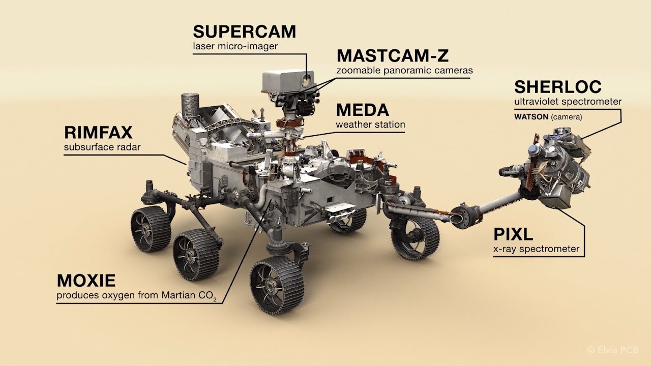
After Mars InSight’s seismometer, SEIS, our talented teams in ELVIA LOIRE VALLEY – CIRETEC took part in the development of Perseverance Rover’s SuperCam.

Was there life on Mars?

NASA’s Perseverance rover landed on the Red Planet on February 18 to get some answers. And to write this new chapter of space exploration, NASA could count on France’s support and its technological skills to develop an essential tool: SuperCam, the very laser camera analyzing the organic and chemical composition of the surface of Mars.

Being a space and aeronautics expert, ELVIA LOIRE VALLEY – CIRETEC has been part of this adventure alongside the Laboratoire d’astrophysique de Bordeaux (LAB), the National Center for Scientific Research (CNRS) and the company Steel Électronique. Our expertise in printed circuit board, including multilayer HDI (High density Interconnect) PCB (Printed Circuit Boards), has been our strength to take up the technical and technological challenges that have arisen in this exploration. This is how we developed several of the SuperCam’s electronic mounts, which are currently used on Mars.

InSight (credits JPL NASA)

We worked on this French technological mission for 4 years, developing cutting-edge technology for the SuperCam. That being said, it was not a first for ELVIA LOIRE VALLEY – CIRETEC, since we also designed some printed circuit boards for the lander InSight’s (INterior exploration using Seismic Investigations, Geodesy and Heat Transport) seismometer SEIS (the Seismic Experiment for Interior Structure). That project has been on Mars since November 26, 2018, and measures the tectonic activity of the planet to deduce information like the size of its core or the thickness of its mantle.

Space and Mars remain full of mysteries for us to solve, and our teams are ready to tackle them.

This means we’ll see you soon for a follow-up on ELVIA PCB GROUP’s space adventure!


The only HITACHI UV/CO2 laser drilling in France is in elvia PCB

By Uncategorized No Comments

The only HITACHI UV/CO2 laser drilling in France is in elvia PCB!

Nowadays, High Density Interconnected PCBs can be manufactured thanks to the creation of µvias. Today, in France, there is just one equipment able to drill those specific vias with extreme accuracy and efficiency. It is called the HITACHI UV/CO2 laser drilling and it is in elvia PCB Group’s factory, in Coutances!

How does it work? The goal is to drill a small via (70 to 180 µm) between a layer N and a N-1. A UV laser source, which drills the top copper (generally between 9 and 17 µm thick), is associated with the CO2 laser source, which comes next to remove the dielectric without damaging the lower copper.

This equipement can be used for laser drilling, but also for cavities laser cleaning, thin layer cutting or flex cutting.

HITACHI UV/CO2 has specific characteristics. The holes minimum diameter enabled by this equipment is of 70 µm with a positioning accuracy of 10 µm. It has an automatic loader and unloader and can work with a maximum panel size of 630 x 530 x 7 mm. And the French exclusivity is that it uses UV (λ =355 nm) and CO2 (λ = 9400 nm) laser sources.


Elvia Printed Circuit Boards

Siège social
ELVIA Printed Circuit Boards
Avenue d’Ochsenfurt,
50200 Coutances

Elvia Printed Circuit Boards