All Posts By

Céline Giron

The only HITACHI UV/CO2 laser drilling in France is in elvia PCB

By Uncategorized No Comments

The only HITACHI UV/CO2 laser drilling in France is in elvia PCB!

Nowadays, High Density Interconnected PCBs can be manufactured thanks to the creation of µvias. Today, in France, there is just one equipment able to drill those specific vias with extreme accuracy and efficiency. It is called the HITACHI UV/CO2 laser drilling and it is in elvia PCB Group’s factory, in Coutances!

How does it work? The goal is to drill a small via (70 to 180 µm) between a layer N and a N-1. A UV laser source, which drills the top copper (generally between 9 and 17 µm thick), is associated with the CO2 laser source, which comes next to remove the dielectric without damaging the lower copper.

This equipement can be used for laser drilling, but also for cavities laser cleaning, thin layer cutting or flex cutting.

HITACHI UV/CO2 has specific characteristics. The holes minimum diameter enabled by this equipment is of 70 µm with a positioning accuracy of 10 µm. It has an automatic loader and unloader and can work with a maximum panel size of 630 x 530 x 7 mm. And the French exclusivity is that it uses UV (λ =355 nm) and CO2 (λ = 9400 nm) laser sources.


PCB TECHNOLOGY TRAINING

By Uncategorized No Comments

PCB Technology training

Designing a printed circuit board is not something that can be improvised and manufacturing it neither. All starts with a mutual recognition of the respective constraints.

Once again, employees from several THALES sites, from different business sectors, but whose common thread remains the electronic board, met at Elvia PCB for 2 days, to attend an initiation to the manufacture of printed circuits. The many stages involved in the manufacture of a printed circuit board were detailed, providing the necessary insights to make tomorrow’s designs even more successful.

We thank our partner, THALES group, and our colleague and co-leader, for trusting us for the organization of this 2019 session.


We will be in Munich from November 13th to 16th, 2018 for ELECTRONICA fair

By Uncategorized No Comments

Munich 2018 – International trade fair for the production of electrical components, systems and applications

From November 13th to 16th, 2018, Elvia PCB Group will attend the Electronica fair in Munich, which have been presenting innovations in the electronics sectoro for more than 50 years.
This trade fair takes place every two years, alternating with the Productronica trade fair. Over 73,000 visitors from 80 countries, half of whom are professionals, attend the fair.

Read More

The International Paris Air Show

By Uncategorized No Comments

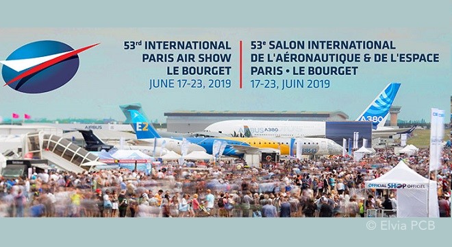
The 53rd edition of the fair will take place at the Bourget Expo Center on 17th to 23rd June 2019.

The Paris Air Show is organised by SIAE, a subsidiary of GIFAS, the French association of Aerospace Industries.
Elvia PCB Group will present its latest technological innovations.
The first 4 days of the fair will be reserved for professionals, followed by 3 days for the general public.

Meet us at NAE pavilion – Hall B2 – Booth D51

Posalux Ultraspeed Trio

By Uncategorized No Comments

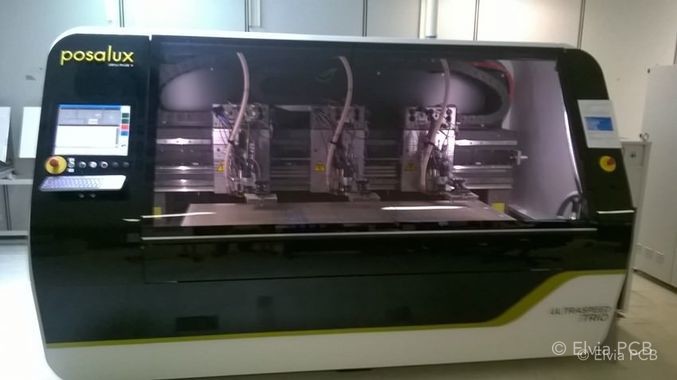
The elvia PCB group, French leader in high-tech printed circuit boards, has invested in a Posalux Ultraspeed Trio at one of its sites, in Coutances (50).

This equipment, equipped with 3 independent camera registration heads, offers new possibilities for high-precision cutting on the 3 axes X, Y and Z and tight tolerances (0.1 mm).

This new machine, complementary to the current equipment, allows us to target new markets such as microwave and medical.

Elvia Printed Circuit Boards

Siège social
ELVIA Printed Circuit Boards
Avenue d’Ochsenfurt,
50200 Coutances

Elvia Printed Circuit Boards